

In the high-stakes arena of microelectronics, the difference between a market-leading processor and a wasted silicon wafer often comes down to a single molecule. As the global semiconductor industry pivots toward sub-5nm architectures and AI-driven hardware, Ultrapure Water (UPW) has transitioned from a basic utility to a critical strategic asset.
For international stakeholders in the water treatment sector, understanding the evolution of UPW is no longer just about chemistry—it is about ensuring the resilience of the global digital supply chain.
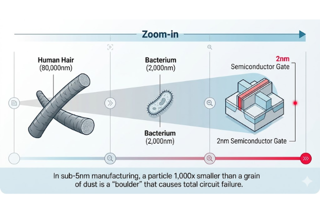
The Precision Paradox: When “Pure” is a Contaminant
In the world of advanced lithography, standard purified water is considered “dirty.” As circuit densities increase, the sensitivity of the manufacturing process reaches a molecular level.
To achieve high-yield production, UPW must be stripped of virtually all ions, silica, and organic carbons (TOC). Even a microscopic particle, invisible under standard magnification, can act as a catastrophic obstruction during the Chemical Mechanical Planarization (CMP) process. For overseas manufacturers and investors, the message is clear: Water quality is the ultimate gatekeeper of chip yield. Failure to maintain 18.2 MΩ·cm resistivity doesn’t just result in defects; it results in millions of dollars in lost throughput.
The Role of UPW in the 2nm Era: Immersion and Integration
We are entering the era of Extreme Ultraviolet (EUV) Lithography and advanced immersion techniques. Here, UPW serves a dual purpose. Beyond acting as the world’s most efficient cleaning solvent, it functions as a refractive medium. By replacing the air gap between the lens and the wafer with high-purity water, manufacturers can achieve a higher numerical aperture, allowing for finer resolution of circuits. This technical requirement has turned water treatment specialists into essential partners in the R&D process of the world’s leading foundries.
The Sustainability Frontier: Balancing Purity and ESG
The greatest challenge facing the industry today is the Water-Energy-Nexus. Producing UPW is inherently resource-intensive. As global ESG (Environmental, Social, and Governance) mandates tighten, the microelectronics industry faces a paradox: How do you increase water purity while decreasing environmental impact?
The focus has shifted toward Circular Water Economies. Leading-edge facilities are now integrating:
- High-Recovery RO Systems: To minimize brine waste.
- Advanced Reclaim Loops: Recycling up to 90% of process water back into the UPW makeup stream.
- Energy-Efficient Deionization: Utilizing next-generation Electrodeionization (EDI) to reduce the carbon footprint of the treatment plant.
Bridging the Gap: The Convergence of Technology and Scale
For the international water treatment community, the rapid expansion of semiconductor “Mega-fabs” represents a unique opportunity for cross-border collaboration. The complexity of these systems requires a synergy of membrane technology, ion exchange resins, and real-time analytical monitoring that can only be achieved through a globalized supply chain.
Join the Global Dialogue at WATERTECH 2026
The future of microelectronics is being written in the purity of its water. As we navigate the complexities of semiconductor manufacturing, the need for innovative, sustainable, and scalable water solutions has never been more urgent.
To discover the latest breakthroughs in UPW technology and connect with the engineers and companies leading the semiconductor water revolution, we invite you to join us at WATERTECH. This is the premier platform for overseas professionals to engage with the Asian market, source cutting-edge components, and witness the future of industrial water treatment.
- Date: June 9-11, 2026
- Venue: National Exhibition and Convention Center (NECC), Shanghai
- Registration: Open now for international visitors.
Secure your place at the center of the world’s most dynamic water technology hub. We look forward to seeing you in Shanghai.
